
二維度電子元件的製備與特性鑑定
Fabrication and characterization of two dimensional electronic devices
國立臺灣大學光電創新中心 陳奕君 教授
中央研究院物理所 李偉立 副研究員
計畫執行期間:2021.1.1 – 2022.12.31
優良研究成果
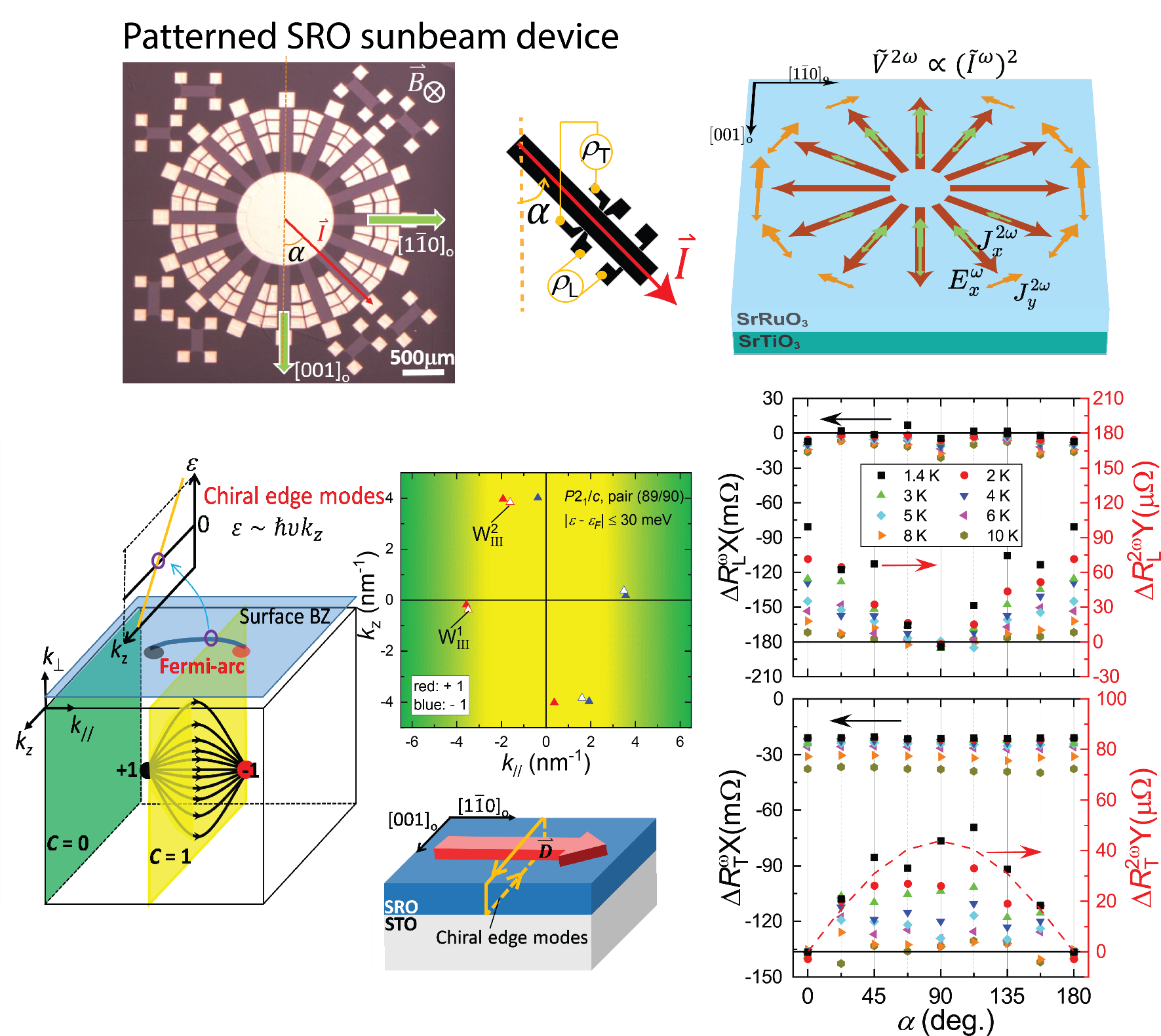
Revealing topological surface states via nonlinear and nonreciprocal transport effects
One of the challenging subjects in topological systems is to identify the charge transport signatures associated with the unusual surface states due to nontrivial band topology. In a recent international collaborating work partly funded by a joint project of Academia Sinica and National Taiwan University, unusually large nonreciprocal and nonlinear charge transport effects (NRTE) in both longitudinal and transverse channels were observed in thin films of topological ferromagnetic Weyl metal SrRuO3 (SRO). These behaviors align with a proposed scenario of an effective Berry curvature dipole originating from Fermi-arc surface states accompanied by 1D chiral edge modes, which is supported by electronic band structure calculations. Our findings not only highlight the significance of NRTE as a charge transport probe for topological surface states with a broken inversion symmetry but also feature potential applications in nonreciprocal electronics and nonlinear optics using topological materials. The complete data and analyses have been recently accepted for publication at Physical Review X 14, 011022 (2024) (https://link.aps.org/doi/10.1103/PhysRevX.14.011022 ).
The SRO thin film growth, device fabrication, and transport measurements were carried out by Dr. Wei-Li Lee’s group at IoPAS and Prof. I-Chun Cheng’s group at NTU supported by a joint project of Academia Sinica and National Taiwan University. The electronic band structure calculations were performed by Prof. Guan-Yu Guo’s group at NTU and Prof. Wei-Cheng Lee’s group at SUNY Binghamton. The optical SHG measurements were performed by Prof. David Hsieh’s group at Caltech. The SRO thin film structural characterizations were performed by Director Chia-Hung Hsu’s group at NSRRC.
High-mobility 2D WS2 field-effect transistor with Bi/Au contacts
Transition metal dichalcogenides (TMDs) are distinguished by their layered structure, characterized by robust covalent bonds in the in-plane direction and weaker van der Waals bonds in the out-of-plane direction. These materials exhibit excellent electronic properties, including wide bandgap, high mobility, and efficient electrostatic control, rendering them suitable for applications in semiconductor devices such as field-effect transistors, solar cells, photodetectors, and p-n diodes. In our collaborative research endeavor, we successfully demonstrated high-mobility back-gated 2D WS2 field-effect transistors without the need for intentional doping, annealing, or the incorporation of buffer layers. The WS2 flake was prepared by the mechanical exfoliation method. The thickness of the WS2 active layer was around 3.9 nm. To effectively mitigate contact resistance, we employed Bi/Au contacts. The absence of discernible current crowding in the output characteristics suggests that the contact between WS2 and Bi/Au manifests ohmic behavior. At room temperature, our WS2 field-effect transistor exhibited an on/off current ratio of ~105, a subthreshold swing of 1.25 V/dec, and a field-effect mobility of 103 cm2V-1s-1. At lower temperatures, an increase in the on current was observed, attributed to phonon scattering dominating the band-like transport in WS2. At 5 K, an impressive mobility of 562 cm2V-1s-1 was achieved. This performance stands on par with, or even surpasses, that of reported WS2 transistors incorporating doping, annealing, or additional buffer layers. This significant achievement was recognized with the “Best Oral Paper Award” at the “International Electron Devices & Materials Symposium 2023.”
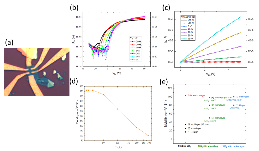
Figure (a) Optical micrograph, (b) temperature-dependent transfer characteristics, (c) room-temperature output characteristics, and (d) temperature-dependent mobility of back-gated 2D WS2 field-effect transistor with Bi/Au contacts. (e) Comparison of room-temperature mobility for various WS2 field-effect transistors.