
室溫量子自旋電子與聲子的媒合
Marriage of quantum spintronics and phononics at room temperature
In this project, we have ultilized the various techniques and experties of all PIs and co-PIs to develope the new research area of thermal transport on non-magnetic and magnetic nanowires. For the growth of magnetic nanowire of Mn-SiGe, we established a new method to introduce Mn gas precursors MnCl2 during the VLS nanowire growth in CVD, such that Mn and Si atoms could be absorbed from the vapor phase by the Au-Si liquid catalysts and co-precipitated to form Si-Mn alloy nanowires. For the thermal transport probe, we have developed a new and sensitive probe based on the concept of thermal rectification. The thermal rectification in a pristine SiGe nanowire is shown in the inset of Fig. 1(a). The 4ω signals display a non-zero background which decreases with increasing Is,DC (or Ts,DC) as shown in Fig. 1(a). Regardless of the presence of the background, the absence of a peak at Is,DC=16μA indicates that there is no thermal rectification (R-1<0.2%). The result can be further verified by measuring 1ω and 2ω signals described above. As shown in Fig. 1(b), the 1ω/2ω signals vs. Ih,DC display a linear relation without a bump, which consistently indicate R-1<0.2% in the SiGe nanowire.
For the non-magnetic crystalline nanowire, Bi2-xSbxTe3 (BST) nanowires were grown directly from Bi0.5Sb1.5Te3 thin film by thermal annealing and the diameter dependence of thermoelectric properties of single BST NW has been in-situ studied in FIB trimming. The consequence implies the size and defect effects have more influence on phonon scattering than that of electron carriers in this diameter region. When the NW was further trimmed to 285 nm, both the electrical and thermal conductivities started a dramatic drop due to the formation of a large number of defects and the amorphous-like structure. The study not only provides the thoroughly understanding of the size and ion irradiation effects on the electrical and thermal transport properties but also provides a possible method to manipulate the physical properties in nanostructures for the extensive applications in engineering high ZT thermoelectric materials.
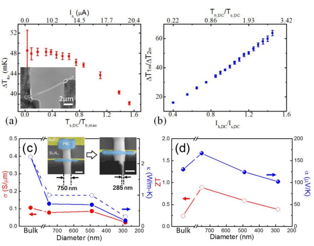 FIG. 1. (a) The signals at 4ω of a SiGe nanowire when gradually raising the Ts,DC of the sensor. The inset shows the SEM image of the SiGe nanowire anchored between a heater and a sensor. (b) The 1ω/2ω signals of the same sample when gradually raising the Th,DC of the heater. From the data and our analyses, we determine R-1<0.2%. (c), (d) The diameter dependent electrical, thermal conductivity, seebeck coefficient and figure of merit and of a FIB trimmed BST nanowire.
In the near future, we will further use this technique to explore the dynamic magnetism and the thermal properties of for the quasi-one dimensional magnetic nanowires.
本計劃中我們研究了摻雜錳元素於矽奈米線以將其變成磁性半導體的可能性,並探討了各種奈米線的熱傳導與熱整流性質。在生長磁性奈米線方面,我們提出了使用氣態MnCl2作為參與Au-Si液態催化反應以析出Si-Mn合金的方法。在熱傳導與熱整流性質的研究上,我們發明了利用4ω方法研究了諸多奈米線的熱整流性質。由於此新方法排除了以往量測熱功率的不確定性,因此比以前的方法更靈敏約十倍(如圖一a所示)。另外我們也開發了1ω/2ω的量測方法,並實驗證實這兩種方法得到一致的結果(如圖一b所示)。以圖一的矽鍺奈米線為例,我們的實驗結果確認其熱整流效應小於0.2%。這個實驗方法將對於介面與非對稱結構上的聲子與熱傳導研究有基礎的重要性。未來我們將利用本計劃所開發的技術與方法研究準一維磁性奈米線並探索基礎的動態磁學與熱傳導問題。
對於非磁性結晶納米線方面,Bi2-xSbxTe3(BST)奈米的成長以通過熱處理技術,直接從Bi0.5Sb1.5Te3薄膜生長,並且整合FIB修剪技術對單根BST NW的熱電性能的原位研究技術探究其物理特性與奈米線直徑之相依性。 結果顯示:尺寸和缺陷效應對聲子散射的影響比在該直徑區域中的電子載流子的影響更大,當NW修剪至285nm時,由於形成大量缺陷和非晶狀結構,電導率和熱導率開始顯著下降。 該研究不僅提供了對尺寸和離子輻射效應對電和熱傳輸性能的徹底理解,而且提供了操縱納米結構中的物理性質的可能方法,可廣泛應用於高ZT熱電材料。
圖一(a) 以4ω方法量測奈米線的熱整流性質。嵌入圖為懸空的矽鍺奈米線,兩端固定於微米熱傳導量測裝置的電子顯微鏡影像。(b)以1ω/2ω方法量測奈米線的熱整流性質。綜合圖一a與b的結果我們確認其熱整。(c), (d)電,熱導率,塞貝克係數和品質因數(ZT)於FIB修剪後BST納米線及其對直徑的相依性。